- 您现在的位置:买卖IC网 > Sheet目录312 > AT27C516-70JI (Atmel)IC OTP 512KBIT 70NS 44PLCC
AT27C516
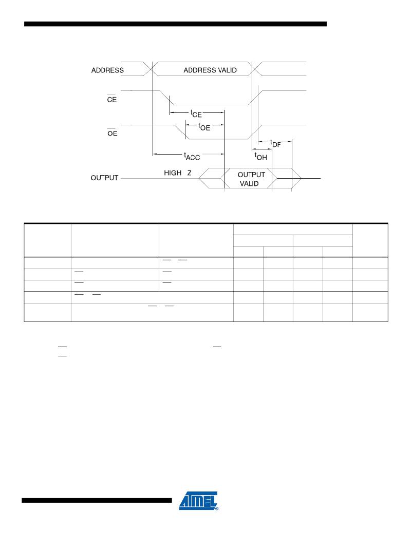
9. AC Waveforms for Read Operation (1)
10. AC Characteristics for Read Operation
AT27C516
-45
-70
Symbol
(3)
t ACC
t CE (2)
t OE (2)(3)
Parameter
Address to Output Delay
CE to Output Delay
OE to Output Delay
Condition
CE = OE = V IL
OE = V IL
CE = V IL
Min
Max
45
45
20
Min
Max
70
70
25
Units
ns
ns
ns
t DF (4)(5)
t OH
OE or CE High to Output Float, whichever occurred first
Output Hold from Address, CE or OE, Whichever
Occurred First
7
20
7
25
ns
ns
Notes:
1. Timing measurement reference level is 1.5V for -45 devices. Input AC drive levels are V IL = 0.0V and V IH = 3.0V. Timing mea-
surement reference levels for all other speed grades are V OL = 0.8V and V OH = 2.0V. Input AC drive levels are V IL = 0.45V
and V IH = 2.4V.
2. OE may be delayed up to t CE - t OE after the falling edge of CE without impact on t CE .
3. OE may be delayed up to t ACC - t OE after the address is valid without impact on t ACC .
4. This parameter is only sampled and is not 100% tested.
5. Output float is defined as the point when data is no longer driven.
5
0362E–EPROM–1/08
发布紧急采购,3分钟左右您将得到回复。
相关PDF资料
AT27LV010A-70JU
IC OTP 1MBIT 70NS 32PLCC
AT27LV020A-12JU
IC OTP 2MBIT 120NS 32PLCC
AT27LV040A-90JU
IC OTP 4MBIT 90NS 32PLCC
AT27LV256A-90JU
IC OTP 256KBIT 90NS 32PLCC
AT27LV512A-90JU
IC OTP 512KBIT 90NS 32PLCC
AT27LV520-90XI
IC OTP 512KBIT 90NS 20TSSOP
AT28BV256-20SU
IC EEPROM 256KBIT 200NS 28SOIC
AT28BV64-30TI
IC EEPROM 64KBIT 300NS 28TSOP
相关代理商/技术参数
AT27C516-70VC
功能描述:IC OTP 512KBIT 70NS 40VSOP RoHS:否 类别:集成电路 (IC) >> 存储器 系列:- 标准包装:32 系列:- 格式 - 存储器:闪存 存储器类型:FLASH 存储容量:1M (128K x 8) 速度:120ns 接口:并联 电源电压:2.7 V ~ 3.6 V 工作温度:0°C ~ 70°C 封装/外壳:32-LCC(J 形引线) 供应商设备封装:32-PLCC 包装:管件 其它名称:AT49BV00112JC
AT27C516-70VI
功能描述:可擦除可编程ROM 512Kb (32Kx16) OTP 5V 70ns RoHS:否 制造商:Maxim Integrated 类型: 存储容量:1024 bit 组织:1 K x 1 接口类型: 工作电流:5 uA 编程电压: 工作电源电压:2.8 V to 6 V 最大工作温度:+ 85 C 安装风格:Through Hole 封装 / 箱体:TO-92
AT27C51685JC
制造商:Atmel Corporation 功能描述:
AT27C516-85JC
功能描述:IC OTP 512KBIT 85NS 44PLCC RoHS:否 类别:集成电路 (IC) >> 存储器 系列:- 标准包装:32 系列:- 格式 - 存储器:闪存 存储器类型:FLASH 存储容量:1M (128K x 8) 速度:120ns 接口:并联 电源电压:2.7 V ~ 3.6 V 工作温度:0°C ~ 70°C 封装/外壳:32-LCC(J 形引线) 供应商设备封装:32-PLCC 包装:管件 其它名称:AT49BV00112JC
AT27C520-70XC
制造商:Atmel Corporation 功能描述:EPROM OTP 512KBIT 64KX8 70NS 20TSSOP - Rail/Tube
AT27C520-90SC
功能描述:IC OTP 512KBIT 90NS 20SOIC 制造商:microchip technology 系列:- 包装:管件 零件状态:停產 存储器类型:非易失 存储器格式:EPROM 技术:EPROM - OTP 存储容量:512Kb (64K x 8) 写周期时间 - 字,页:- 访问时间:90ns 存储器接口:并联 电压 - 电源:4.5 V ~ 5.5 V 工作温度:0°C ~ 70°C(TC) 安装类型:表面贴装 封装/外壳:20-SOIC(0.295",7.50mm 宽) 供应商器件封装:20-SOIC 基本零件编号:AT27C520 标准包装:37
AT27C520-90XC
制造商:Atmel Corporation 功能描述:EPROM OTP 512KBIT 64KX8 90NS 20TSSOP - Rail/Tube
AT27C800-12JC
功能描述:IC OTP 8MBIT 120NS 44PLCC 制造商:microchip technology 系列:- 包装:管件 零件状态:停產 存储器类型:非易失 存储器格式:EPROM 技术:EPROM - OTP 存储容量:8Mb (1M x 8,512K x 16) 写周期时间 - 字,页:- 访问时间:120ns 存储器接口:并联 电压 - 电源:4.5 V ~ 5.5 V 工作温度:0°C ~ 70°C(TC) 安装类型:表面贴装 封装/外壳:44-LCC(J 形引线) 供应商器件封装:44-PLCC(16.59x16.59) 基本零件编号:AT27C800 标准包装:27
